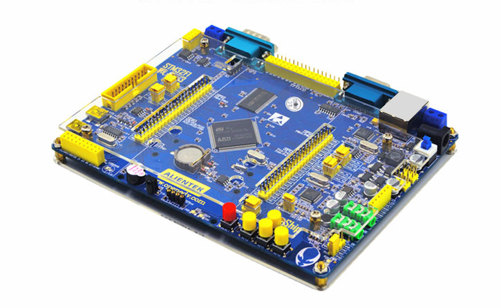
The microcontroller is limited by the storage medium and cannot further process the sent and received data. Therefore, in applications that require further processing of large amounts of data, the powerful data processing capabilities of microcomputers must be used. In this way, reliable data transmission between the PIC microcontroller and the microcomputer must be achieved through communication circuits. The PICl6F876 microcontroller does not provide a serial port, but it integrates two different types of serial communication modules, namely the universal synchronous/asynchronous receiver-transmitter USART module and the master synchronous serial port MSSP. Considering that the serial ports of the PC are all nine-pin 232 structures, the serial interface of the PC is an external bus standard interface that complies with the EIA RS-232C specification. RS-232C uses negative logic, that is, logic “1”: -5v ~ -15v; logic “0”: 5V ~ 15V. The CMOS level is logic “1”: 4.99V, logic “0”: 0.01V; the logic “1” and “0” of TTL level are 2.4V and 0.4V respectively. Therefore, when using the RS-232C bus for serial communication, an external circuit is required to achieve level conversion. The driver is used at the transmitting end to convert the TTL or CMOS level to the RS-232C level, and the receiver is used at the receiving end to convert the RS-232C level into the TTL or CMOS level [2].
MAX232CPE of MAXIM Company is selected here for level conversion. MAX232CPE is a universal serial receiving/transmitting driver chip of MAXIM Company. It is used to realize the level conversion of handshake protocol required when the microcontroller and PC exchange data. The peripheral circuit of MAXIM232 is very simple. It only needs to connect a few external 0.1μF capacitors. The protection resistors between the same network labels are all 330Ω. Therefore, we mainly apply the USART in asynchronous transmission mode. Moreover, serial communication must be implemented using existing communication modules and combined with self-designed communication software.

The core of the USAR asynchronous transmitter is the transmit shift register TSR and the transmit buffer TXREG. TXREG is directly connected to the internal data bus and is a software-readable/writable register. The user program writes the data to be sent into TXREG, and then the hardware automatically controls the data to be loaded from TIREG to TSR (if 9-bit is selected) format, and together with the TX9D bit from TXSTA to form 9-bit data); then automatically add a start bit 0 in front and a stop bit 1 in the back to form a complete frame structure: Finally, in the baud rate clock Under the control of the shift register TSR, the data is sent out bit by bit; completing the conversion of “parallel to serial”.
TSR waits until the stop bit of the data currently being sent is sent out before loading new transmission data from TXREG. Once TXREG sends data into TSR, register TXREG becomes vacated, and at the same time, transmit interrupt flag bit TXIF is set to 1, sending an interrupt request to the CPU. Although the transmit interrupt enable bit TXIE controls whether the CPU responds to the interrupt, TXIF will be automatically set to 1 as long as TXREG is vacated. Moreover, the hardware will automatically clear TXIF only after new transmit data is written to the register TXREG. 0. Therefore, it also provides new ideas and possibilities for us to use software to judge working status.
The core of the USART asynchronous receiver is the receive shift register RSR and the receive register RCREG. The asynchronous serial data sent from the communicating party is input from the RC7/RX/DT pin; under the control of the sampling timing signal provided by the baud rate generator, the data detection and recovery circuit samples the input signal waveform. To restore the original appearance of the data; then, under the control of the shift clock pulse provided by the baud rate generator, the recovered serial data, as well as the start bit and stop bit, are moved into the RSR register step by step.
As long as the stop bit is sampled, the receive shift register RSR loads the received 8-bit data into the receive register RCREG (if RCREG is empty); and loads the 9th bit (if any) into the RX9D bit; completed at the same time “Serial to parallel” conversion; set the receive interrupt request flag bit RCIF=1 to notify the CPU to read the data in the receive register RCREG and the 9th bit data RX9D. In the software design, the 9th bit data is judged (characterized) In terms of data properties, 1 represents the address code and 0 represents the data code) to implement corresponding processing.
Among them, RCREG is a double buffer register with a 2-level structure of first-in-first-out queue. Likewise, the RX9D bit is also a level 2 structure. Therefore, this allows the shift register to receive 2 consecutive frames of data and load them into the queue for buffering, and then the third data can be shifted into the RSR register.
Keywords: wireless data transmission